
INTRODUCTION:
In the modern world, electronics have become an essential part of our lifestyle, making daily tasks easier and more efficient. At the heart of these electronic devices are microchips, which form the backbone of modern technology. However, in manufacturing these chips, engineers face fundamental physical limitations. The patterns carved onto a chip depend on the resolution of optical systems, which is directly related to the wavelength of light—shorter wavelengths allow finer and more precise patterns. Traditional lithography methods reached a point where they could no longer shrink transistor sizes further, making it increasingly difficult to improve chip performance.
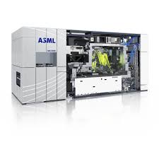
To understand this challenge, imagine trying to draw lines 10,000 times thinner than a human hair—this is the scale required in modern chip fabrication. To overcome this barrier, ASML developed Extreme Ultraviolet (EUV) lithography, a groundbreaking technology that operates at a wavelength of about 13.5 nanometers. These highly advanced machines generate plasma-based light and operate in a vacuum environment to project extremely complex circuit patterns onto silicon wafers with extraordinary precision. This innovation enables the production of ultra-dense, high-performance microchips that power modern computing, artificial intelligence, and advanced communication technologies. ASML’s contributions are vital in meeting the demands of future technology.
HISTORY:
We hear that “every innovation comes from a need,” and this idea perfectly explains the rise of EUV (Extreme Ultraviolet) machines. As the demand for higher computing power increased, engineers faced a serious challenge: how to make chips smaller while improving performance and reducing energy consumption. Early computers were bulky, inefficient, and power-hungry, making miniaturisation essential. The breakthrough came when pioneers such as Jack Kilby and Robert Noyce introduced the integrated circuit, which allowed multiple components to be placed on a single chip. This innovation laid the foundation of modern electronics, but as demand kept growing, shrinking transistors further became increasingly difficult due to physical and technological limits.
These limitations pushed engineers to innovate beyond traditional methods, leading to advanced lithography techniques. One of the most significant breakthroughs is EUV lithography, which uses extremely short-wavelength light to create ultra-fine circuit patterns on silicon wafers. A major contributor to this technology is ASML, which played a crucial role in turning EUV into reality. Their innovation has allowed the semiconductor industry to continue shrinking chip sizes while boosting performance, powering modern processors used in smartphones, artificial intelligence, and communication systems. Today, EUV technology stands as a symbol of human ingenuity, proving that challenges often lead to the most revolutionary advancements.
INNOVATION:
The development of EUV lithography by ASML stands as one of the most complex and collaborative engineering achievements in modern technology. It was driven by an urgent need to overcome the physical limits of traditional chip manufacturing. As transistor sizes approached the nanometer scale, conventional photolithography methods began to fail because resolution is fundamentally limited by the wavelength of light. To continue scaling, engineers explored the use of much shorter wavelengths—around 13.5 nanometers—to etch finer patterns onto silicon wafers.
However, this solution introduced a new set of extreme challenges. EUV light does not naturally exist in a stable, usable form, is almost entirely absorbed by air, and cannot pass through conventional optical lenses. This meant that entirely new technologies had to be invented, including vacuum environments and advanced reflective mirror systems. What once seemed nearly impossible for large-scale industrial use eventually became a reality through decades of innovation, collaboration, and persistence, transforming the future of semiconductor manufacturing.
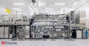
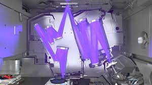
To overcome these extreme challenges, multiple companies and scientists came together in a remarkable display of collaboration. Cymer developed an innovative method to generate EUV light by firing microscopic droplets of tin into a vacuum chamber and striking them with high-energy lasers supplied by TRUMPF. This process creates an extremely hot plasma that emits EUV radiation, which is then used to form ultra-fine patterns on silicon wafers. Generating such light requires not only advanced technology but also perfect timing and synchronization at every step.
At the same time, guiding this EUV light required revolutionary optics. Carl Zeiss AG engineered ultra-precise mirrors with atomic-level smoothness to accurately reflect and direct the light, since traditional lenses cannot be used. The entire system operates in a near-perfect vacuum to prevent absorption and contamination, demanding breakthroughs in vacuum engineering and system stability. Adding to this complexity, tin droplets travel at speeds of around 8–12 m/s and are struck by lasers within fractions of a second—each droplet being hit multiple times with extreme precision. This level of synchronization, speed, and accuracy makes EUV lithography one of the most extraordinary engineering achievements in modern history.
The research and development behind EUV lithography required massive financial investment, running into billions of dollars. Leading semiconductor companies like Intel, TSMC, and Samsung Electronics played a crucial role by funding and supporting this innovation. They invested heavily in testing early prototypes and refining the technology, helping transform EUV machines from experimental concepts into reliable systems capable of mass chip production.
These investments were not just expenses—they were strategic moves that ultimately benefited the companies themselves. By enabling the production of smaller, faster, and more efficient chips, EUV technology accelerated their growth and strengthened their leadership in the semiconductor industry. In the end, their willingness to invest in such a challenging and uncertain technology paid off, shaping the future of modern computing.
IMPACT ON WORLD:
The modern world has been truly transformed by the impact of EUV lithography developed by ASML which enabling the production of extremely small, faster, and more energy-efficient microchips that power almost every aspect of today’s digital life also This breakthrough has played a crucial role in sustaining Moore’s Law, which predicts the exponential increase in the number of transistors on a chip, thereby continuously improving computing performance. By enabling semiconductor leaders such as Intel, TSMC, and Samsung Electronics to manufacture chips at nanometer scales, EUV has accelerated advances in artificial intelligence, high-speed communications, cloud computing, and scientific research.
KNOW MORE:
INTERNAL LINKS:
https://techman.live/android-vs-ios-mobile-which-one-better-for-you-in-2025/
https://techman.live/top-8-tech-gadgets2026/
EXTERNAL LINKS:
https://en.wikipedia.org/wiki/Extreme_ultraviolet_lithography