
INTRODUCTION:
Our lives have become more comfortable, convenient, and efficient with the help of countless electronic devices. From smartphones that allow us to communicate with anyone around the world within seconds and laptops that provide access to unlimited information with just a few clicks, to smartwatches that monitor our heartbeats and count our steps in real time, technology has transformed the way we live. Cars have replaced traditional horse-drawn carriages, making transportation faster and more comfortable. Smart TVs allow us to enjoy high-quality videos and movies, while air conditioners keep our rooms cool even during the hottest days. These are just a few examples of the countless devices that have become an essential part of our daily lives. But have you ever wondered how humanity evolved from living in primitive tribes to creating such extraordinary technologies? What makes these devices so intelligent, powerful, and efficient? What allows a smartphone to process billions of operations in seconds or a smart TV to stream high-quality videos instantly?
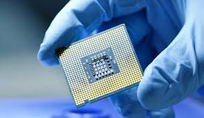
The answer lies in one of the most revolutionary inventions of the modern era: semiconductors. Hidden inside tiny microchips, semiconductors are the foundation of almost every electronic device we use today. Often called the “brain of electronic devices,” they control the flow of electricity through circuits and enable billions of calculations every second. Without them, modern technologies such as artificial intelligence, cloud computing, smartphones, electric vehicles, advanced medical equipment, and even space exploration would be impossible. But how can such extraordinary technology be created from a simple material like silicon? How do semiconductors actually work, and what makes them one of the most valuable technologies on Earth? In this article, we will explore the fascinating world of semiconductors, from their basic principles and historical development to their revolutionary role in powering our digital world and shaping the future of innovation.
HISTORY:
The history of semiconductors dates back to the late 19th century, long before the modern electronic world. During this period, scientists discovered that different materials behaved differently when electricity passed through them. Some materials, known as conductors, allowed electricity to flow freely, while others, called insulators, resisted the flow of electric current. However, scientists were fascinated by a third category of materials that sometimes behaved like conductors and sometimes like insulators. Scientists called these materials semiconductors because their electrical conductivity lies between that of conductors and insulators. This unusual behaviour raised many questions among scientists, encouraging them to investigate their properties and discover how they could be controlled and used to develop new technologies. One of the earliest important discoveries came in 1874, when German physicist Karl Ferdinand Braun discovered the rectifying effect in certain crystals. He demonstrated that electric current could flow more easily in one direction than in the opposite direction. This discovery laid an important foundation for the development of future semiconductor-based electronic devices.
As research progressed into the early 20th century, scientists began studying semiconductor materials such as silicon and germanium more deeply because of their unique and controllable electrical properties. Their research eventually led to one of the greatest breakthroughs in technological history. In 1947, at Bell Laboratories, scientists John Bardeen, Walter Brattain, and William Shockley developed the first working transistor. This tiny device could amplify and switch electronic signals, replacing large and inefficient vacuum tubes. The invention of the transistor made electronic devices smaller, faster, more reliable, and energy-efficient. It was a revolutionary achievement that opened the door to a new era of electronics. The innovation continued in the late 1950s when engineers developed the integrated circuit (IC), which allowed multiple electronic components, including transistors, to be placed on a single semiconductor chip. This breakthrough dramatically increased computing power while reducing the size and cost of electronic devices, making the development of modern computers and smartphones possible.
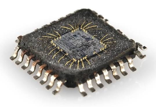
Over the following decades, semiconductor technology advanced at an extraordinary pace. Manufacturers learned how to place thousands, millions, and eventually billions of transistors onto a single microchip. This remarkable progress became closely associated with Moore’s Law, an observation that the number of transistors on a microchip roughly doubles every two years. As a result, electronic devices became increasingly powerful, compact, affordable, and efficient. Today, semiconductors are the backbone of modern technology, powering everything from smartphones, laptops, and smart televisions to artificial intelligence systems, electric vehicles, advanced medical equipment, and spacecraft. What began as a scientific curiosity in the 19th century has become one of humanity’s greatest technological achievements, driving the digital revolution and continuing to shape the future of innovation.
HOW SEMICONDUCTORS WORK:
Now, before understanding how semiconductors work, we first need to understand what makes them so special. A semiconductor is a material whose electrical conductivity lies between that of a conductor, such as copper and iron, and an insulator, such as rubber. However, its real speciality is not simply that it has properties of both conductors and insulators, but that we can precisely control its electrical conductivity. In other words, we can design it to allow or restrict the flow of electric current whenever required. This unique ability makes semiconductors extremely useful in modern electrical and electronic technology. One of the most commonly used semiconductor materials is silicon because it is abundant in nature, relatively inexpensive, reliable, and has excellent electrical properties. But you might wonder: if silicon is so abundant in nature, especially in sand, why don’t we simply extract it and use it directly to conduct electricity? The reason is that silicon in ordinary sand is mainly present in the form of silicon dioxide (SiO₂), chemically bonded with oxygen. Even after extracting and purifying silicon, its electrical behaviour is not suitable for building complex electronic devices without further modification. Scientists solve this problem through a process called doping, in which carefully controlled amounts of other elements are added to silicon to modify its electrical properties and create regions with different characteristics.
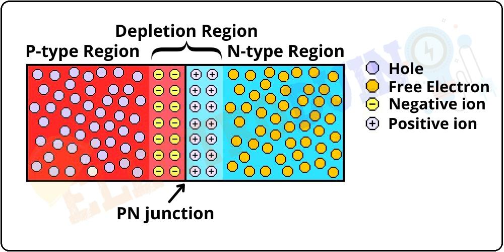
There are two main types of doping: N-type doping and P-type doping. In N-type doping, manufacturers add elements such as phosphorus, arsenic, or antimony, which have five electrons in their outermost shell, also known as valence electrons. Four of these electrons form covalent bonds with neighbouring silicon atoms, while the fifth electron becomes available for electrical conduction. As a result, free electrons become the majority charge carriers, creating N-type silicon. On the other hand, in P-type doping, manufacturers add elements such as boron, which has only three valence electrons. These electrons form three covalent bonds with neighbouring silicon atoms, leaving one bond short of an electron. This creates a vacancy called a hole, which behaves like a positive charge carrier. Holes therefore become the majority charge carriers, creating P-type silicon. Now, things become even more interesting when these two differently doped regions are joined together to form a P-N junction. Electrons from the N-type region begin diffusing towards the P-type region, while holes move in the opposite direction. Near the junction, electrons and holes recombine, leaving behind fixed positively and negatively charged ions. These ions create a region with very few mobile charge carriers, known as the depletion region. The electric field produced by these fixed ions opposes further diffusion and creates a potential barrier. For a typical silicon P-N junction at room temperature, this built-in potential is often around 0.6–0.8 volts, depending on its doping and structure. But what happens when we apply an external voltage? If we connect the positive terminal of a battery to the P-type region and the negative terminal to the N-type region, the depletion region becomes narrower, and the potential barrier decreases, allowing current to flow more easily. This is called forward bias. However, when we reverse these connections, the depletion region becomes wider and the potential barrier increases, restricting current flow. This is called reverse bias. Through these principles, semiconductor devices can control the movement of electrical charges with remarkable precision.
transistor works as an electrically controlled switch or amplifier. By controlling its ON and OFF states, a transistor can represent binary digits: 1 and 0. In simplified digital logic, an ON state represents 1, while an OFF state represents 0. Billions of these microscopic transistors are integrated into modern semiconductor chips, working together to perform calculations and process information. These transistors can switch between states billions of times per second, allowing electronic devices to execute instructions, store information, process images, and run complex software applications. Modern semiconductor chips contain incredibly small transistors, with critical dimensions measured in nanometers. From sending a text message and streaming a video to running advanced artificial intelligence systems, almost every digital activity we perform today depends on the precise control of electrical signals made possible by semiconductor technology.
HOW SEMICONDUCTOR MANUFACTURE:
Now, we come to one of the most complex and extraordinary manufacturing processes ever developed by human beings: semiconductor manufacturing. Imagine building an entire city out of a tiny grain of sand, where billions of transistors act like houses, and each one is connected through an incredibly organised network of roads that allow electricity to flow like vehicles without creating traffic. This remarkable level of precision is made possible by advanced engineering and manufacturing technologies. But how does this extraordinary process begin? Surprisingly, it starts with one of the most abundant materials on Earth: silicon. Yes, the same silicon found in ordinary beach sand and quartz. However, silicon cannot be used directly for chip manufacturing because it is naturally combined with oxygen and other impurities. Therefore, it must first undergo a purification process. Initially, silica (silicon dioxide) is heated with carbon in an electric furnace at temperatures of approximately 2,000°C. During this chemical reaction, carbon removes oxygen from silicon dioxide, producing metallurgical-grade silicon with a purity of approximately 98–99%. Although this is an important first step, semiconductor manufacturing requires silicon of an extraordinarily higher purity, which will be achieved through further refining processes.
SiO2+2C→Si+2CO

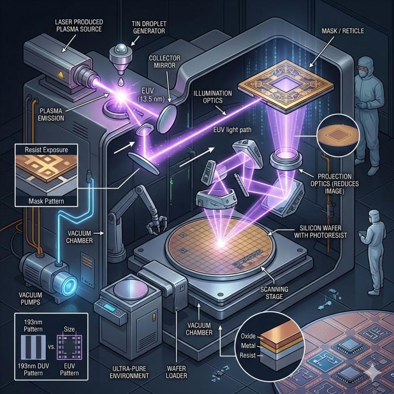
After purifying silicon and modifying its electrical properties through doping, the next step is to transform it into a form that can be used to manufacture semiconductor chips. First, highly purified silicon is melted and grown into a large cylindrical single crystal using a specialised process. This crystal is then carefully sliced into extremely thin, circular discs called silicon wafers. These wafers act as the foundation on which billions of transistors and other microscopic electronic components will eventually be fabricated. Before manufacturing begins, engineers thoroughly clean the wafer to remove dust particles, oil, and other unwanted contaminants. Think of it as preparing a perfectly clean canvas before creating a masterpiece. Once the wafer is ready, a light-sensitive chemical called photoresist is spread evenly across its surface by spinning it at high speed. This creates an extremely thin coating, similar to spreading a photographic film over a blank canvas. The wafer then enters one of the most advanced machines ever developed by humans: an EUV lithography machine. It generates extreme ultraviolet light with a wavelength of just 13.5 nanometres and uses a specially designed patterned plate called a photomask or reticle to transfer microscopic circuit patterns onto the photoresist. Through this incredibly precise process, manufacturers create patterns layer by layer, gradually building the complex structures required for billions of interconnected transistors. After exposure, the wafer undergoes a development process in which a developer solution removes selected portions of the photoresist, depending on whether positive or negative photoresist is used. This reveals the desired circuit pattern on the wafer. Next comes etching, a process that removes unwanted material from the exposed regions using chemical solutions or plasma, transferring the designed pattern into the underlying material. Once etching is complete, the remaining photoresist is removed because it has already served its purpose as a temporary protective mask. These processes are repeated many times, along with other manufacturing steps such as deposition, doping, and polishing, to build the complete semiconductor structures. Finally, the finished wafer is inspected and tested, then cut into individual chips called dies. These dies undergo further testing, and the working ones are packaged and connected to external electrical contacts before being integrated into electronic devices such as smartphones, laptops, and computers.
The entire semiconductor manufacturing process is not completed in a single day. In fact, manufacturing an advanced semiconductor chip can take several months and requires some of the most sophisticated machinery and highly controlled environments ever developed by humans. The result of this incredibly complex process is a tiny microchip containing billions of microscopic transistors, capable of performing billions of operations every second. These powerful chips are the backbone of modern technology, powering everything from smartphones, laptops, and cars to spacecraft and advanced artificial intelligence systems. However, this achievement did not happen overnight. It is the result of decades of continuous research, engineering, and technological innovation. Scientists and engineers are constantly developing new manufacturing techniques to make transistors smaller, improve energy efficiency, increase processing speeds, and pack more computing power into increasingly tiny chips. This continuous advancement is what makes modern semiconductor technology more powerful and efficient with every generation.
IMPACT:
Few technologies in human civilization have been as revolutionary as semiconductors. Although hidden inside almost every electronic device, semiconductor chips have become the foundation of the modern digital world, influencing nearly every aspect of our daily lives. From smartphones and computers to household appliances and advanced machinery, almost every electronic device relies on semiconductors to function. One of their most significant contributions has been the advancement of computing technology. In the 1940s and 1950s, computers were enormous machines that occupied entire rooms, were extremely expensive, and required considerable time to perform calculations. However, the development of semiconductor technology transformed computing by making devices smaller, faster, more affordable, and more efficient. Today, powerful computers can fit in our pockets, delivering vast amounts of information and performing complex calculations within seconds. Thus, semiconductors have completely transformed the way humans access information, communicate, work, and interact with the world.
The contribution of semiconductors extends across several major sectors, including communication, healthcare, and transportation. In communication, semiconductor chips power modern smartphones, internet infrastructure, satellites, and wireless networks, enabling people to connect across the globe and exchange enormous amounts of information within seconds. In healthcare, semiconductors play a crucial role in advanced medical equipment such as CT scanners, X-ray machines, MRI systems, and robotic surgical instruments, helping doctors diagnose diseases more accurately and perform complex procedures with greater precision. Similarly, in transportation, modern vehicles contain hundreds or even thousands of semiconductor chips that control engine performance, navigation systems, safety features, and driver-assistance technologies. These innovations have improved vehicle efficiency, enhanced road safety, and laid the foundation for self-driving cars. Beyond these sectors, semiconductors are also driving emerging technologies such as artificial intelligence, cloud computing, robotics, renewable energy, and space exploration. Powerful AI systems require enormous computing power to process data and train advanced models, while semiconductors enable more efficient solar energy systems, energy storage solutions, and satellite communication networks.
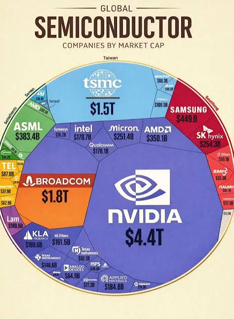
Apart from their technological importance, semiconductors have also become one of the most strategically and economically valuable industries in the world. Countries increasingly recognize that control over semiconductor manufacturing and innovation is essential for economic growth, national security, and technological leadership. As a result, governments are investing billions of dollars in semiconductor research, manufacturing facilities, and infrastructure while encouraging businesses and entrepreneurs to enter this rapidly growing industry. Nations around the world are competing to strengthen their semiconductor capabilities and reduce dependence on foreign chip suppliers. This growing competition highlights how important semiconductors have become to the global economy and the future of technological development. From powering the smallest electronic devices to enabling the most advanced artificial intelligence systems, semiconductors are the invisible engines of the digital age, continuously transforming human civilization and shaping the future of humanity.
CONCLUSION:
The story of modern semiconductors is not a simple one; rather, it is the result of decades of scientific research, technological breakthroughs, and continuous engineering advancements. Through the combined efforts of brilliant scientists and engineers, semiconductors have evolved into incredibly powerful microchips capable of containing billions of transistors within incredibly small spaces. This remarkable progress has transformed the way humans live, work, communicate, and innovate, while laying the foundation of the modern technological world. Today, semiconductors are at the heart of almost every advanced technology, powering everything from smartphones, computers, artificial intelligence systems, medical equipment, and electric vehicles to countless other electronic devices. They are no longer just electronic components but the driving force behind global innovation, industrial development, and economic growth. As emerging technologies such as artificial intelligence, quantum computing, advanced robotics, and space exploration continue to evolve, the demand for faster, smaller, more powerful, and energy-efficient semiconductor chips will continue to grow, making them increasingly essential to shaping the future of humanity.
KNOW MORE:
INTERNAL LINKS:
https://techman.live/what-is-antimatter-the-mysterious-energy-that-could-change-the-future/
https://techman.live/asml-euv-lithography-from-impossible-idea-to-reality/
EXTERNAL LINKS: